header graphics

PCB Layout

header graphics
PCB Design

Precision PCB Layout Services for High-Performance Electronics

Got your schematic ready? Lets turn it to a production ready PCB with accurate component placement and précised routing. With Our PCB Layout Services, we help various industries to create reliable manufacturable PCBs that maximize electrical performance and reduce manufacturing issues. From component placement to signal integrity and thermal management, we build layouts that are reliable, manufacturable, and ready to scale.

Talk to PCB Expert

Our PCB Layout Capabilities

star Precision Component Placement
star High-Speed Signal Routing
star Differential Pair Routing
star Controlled Impedance Layout
star Power & Ground Plane Optimization
star EMI/EMC Optimized Layout
star Thermal Management
star Via Optimization
star BGA Fan-Out Design
star Fine Pitch Routing
star Design Rule Check
Our PCB Layout Capabilities

Build a PCB in which all components gets placed perfectly, every trace gets routed, and your circuit goes from "works on paper" to "works for real.
Our PCB Layout Capabilities

Our PCB Layout Services

star Single Layer PCB Layout
star Double Layer PCB Layout
star Multi-Layer PCB Layout
star High-Speed PCB Layout
star High-Frequency PCB Layout
star HDI PCB Layout
star Flexible PCB Layout
star Rigid-Flex PCB Layout
star RF PCB Layout
star Mixed Signal PCB Layout
OUR PROCESS

PCB Layout Design Flow

1
Review
Schematic Review
Our Engineers start by inspecting your Schematic to understand circuit functionality, design, and manufacturing constraints to create a strong foundation before starting layout
2
Component Placement
We strategically positioned the components to optimize signal flow, thermal performance and manufacturing efficiency to reduce routing complexity while improving PCB reliability.
3
Stack-up Planning
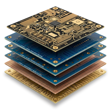
We define the optimal PCB layer stack-up based on your signal, power, and EMI requirements. A well-planned stack-up enhances signal integrity and simplifies manufacturing.
4
Signal Routing
Our team performs clean trace routing while maintaining impedance control, minimizing crosstalk, and reducing interference across the board.
5
Power & Ground Optimization
We carefully design power and ground planes to provide stable voltage distribution, reduce electrical noise, and improve thermal management for better system performance.
6
DRC & Verification
We make sure that your PCB follows all Design Rule Checks (DRC) and engineering verification to identify spacing, clearance, and routing issues before manufacturing, reducing costly revisions.
7
Gerber File Generation
After layout is finalized and verified, we generate an accurate Gerber Files and manufacturing outputs that are ready for PCB assembly and Fabrication with complete documentation.
COMPLIANCE & QUALITY

PCB Layout Standards We Follow

Our PCB Layout Capabilities
IPC

IPC-2221

Generic PCB Design
Standard

IPC

IPC-7351

Land Pattern & Component
Placement

IPC

IPC-A-600

PCB Quality &
Acceptability

IPC

IPC-6012

Rigid PCB Qualification &
Performance

IPC

RoHS

Restriction of Hazardous
Substances

Frequently Asked Questions

 Know Before You Build

Yes, Our Engineers are capable of designing layout for applications that requires strong Signal integrity and reliable board performance. From Impedance routing to stack up planning to EMI reduction techniques, we ensure stable operation in high-speed electronic systems.

Our PCB engineers are familiar with industry leading design tools including Altium Designer, KiCad, Cadence Allegro, OsCAD PCB Designer and Autodesk Eagle.

Yes Absolutely, After your PCB layout is verified and completed, we provide complete manufacturing ready files, including Gerber Files, Drill Files, Pick & Place Files, Assembly Drawings, BOM and other required documents for manufacturing.

Yes, We can help you modify or upgrade your existing schematic. Our engineers reviews the existing design, understand requirements create a professional PCB layout optimized for electrical performance, manufacturability, and reliability

Our team follows IPC standards and best manufacturing practices making PCb fully suitable for both prototype development and large scale production.

The timeline of PCB layout design depends on complexity of your requirements such as the number of layers, design requirements, etc, Though it takes around 2-3 business days for simple PCBs and 1-2 weeks for a high speed complex layout design.

Yes, Our every PCB layout Project undergoes through a DFM review to make sure its free from any manufacturing Issue Before Production to minimize production costs and fabrication errors.

Build précised PCB Layout for your Next Project

Let’s turn your schematic into a clean, precise, manufacturing-ready PCB layout. From component placement and power distribution to better signal flow, we help you get the ideal layout right from the start. Have a schematic ready? Let’s turn it into a PCB layout built for your project.

Discuss your Project